
Semiconductor Electronics: Materials, Devices and Simple Circuits is Chapter 14 of the NCERT Class 12 Physics Part II textbook. It runs about 21 printed pages from page 322 in the 2026-27 reprint, and it is the chapter that explains how the diode — the key building block of electronic circuits — actually works.
The official NCERT PDF of the chapter is right below this paragraph. After it, this page walks through the chapter section by section — energy bands, doping, the p-n junction, the diode, and rectifiers — so the textbook makes sense the first time you read it.
Download the NCERT Class 12 Physics Chapter 14 Semiconductor Electronics PDF
This is the official NCERT edition, the 2025-26 reprint, published on the NCERT website. Opening it gives you the complete chapter exactly as printed — every section from 14.1 to 14.7, the Summary, the Points to Ponder and the end-of-chapter exercises.
Download the NCERT Class 12 Physics Chapter 14 Semiconductor Electronics PDF from the official NCERT textbooks portal on ncert.nic.in, where NCERT publishes the Class 12 Physics Part II books.
| What the chapter holds | Count | Where it is used |
|---|---|---|
| Printed pages | 21 | |
| Sections in the chapter | 10 | |
| Figures with NCERT captions | 29 | |
| Exercise questions | 6 | answered in our NCERT Solutions |
| Official NCERT PDF | Download the chapter PDF | the chapter exactly as NCERT publishes it |
Chapter at a Glance: Sections, Figures and Exercises
The table below lists how much this chapter holds — its sections, figures, worked examples and exercise questions — exactly as they appear in the NCERT Class 12 Physics Part II book.
The table describes this NCERT textbook chapter, not the whole CBSE scheme. The chapter itself moves in a straight line:
- 14.1 Introduction
- 14.2 Classification of Metals, Conductors and Semiconductors
- 14.3 Intrinsic Semiconductor
- 14.4 Extrinsic Semiconductor
- 14.5 p-n Junction
- 14.6 Semiconductor Diode
- 14.7 Application of Junction Diode as a Rectifier
- Summary, Points to Ponder and Exercises
What This Chapter Covers: A Section-by-Section Tour
The chapter builds in a deliberate order — classification, then charge carriers, then the junction, then the diode, then the rectifier. Each section sets up the one that follows it.
| Section | What it establishes | NCERT pages |
|---|---|---|
| 14.1 Introduction | Why solid-state devices replaced bulky vacuum tubes or valves | 322–324 |
| 14.2 Classification | Resistivity ranges and the energy band picture of solids | 324–326 |
| 14.3 Intrinsic semiconductor | Covalent bonds, the hole, and why \( n_e = n_h = n_i \) | 327–329 |
| 14.4 Extrinsic semiconductor | Doping, donors and acceptors, n-type and p-type materials | 329–332 |
| 14.5 p-n junction | Diffusion, drift, the depletion region, barrier potential | 333–334 |
| 14.6 Semiconductor diode | Forward and reverse bias, V-I characteristics, dynamic resistance | 334–337 |
| 14.7 Rectifier | Half-wave and full-wave rectifiers, capacitor filter | 338–340 |
| Summary and Points to Ponder | The chapter’s own takeaways and its explicit warnings | 340–341 |
| Exercises | Concept checks on every major idea | 341–342 |
The chain of reasoning runs: section 14.2 classifies materials, 14.3 and 14.4 create the two carrier types, 14.5 joins them into a junction, 14.6 shows how the junction conducts, and 14.7 puts the diode to work turning ac into dc. Miss one link and the next section feels unexplained.
Key Concepts: How the Chapter Builds from Energy Bands to a Rectifier
Six ideas carry the whole chapter. Each block below opens with what the idea is and why the chapter needs it, then gives the formulas and page references.
Conductivity and energy bands
A solid conducts only if electrons can reach its conduction band. The energy gap \( E_g \) between the top of the valence band and the bottom of the conduction band is what decides this (NCERT, p. 325).
The chapter classifies solids by resistivity first (NCERT, p. 324):
| Material | Resistivity \( \rho \) | Energy gap \( E_g \) |
|---|---|---|
| Metals | \( 10^{-2} \) to \( 10^{-8}\ \Omega\ \text{m} \) | \( \approx 0 \) |
| Semiconductors | \( 10^{-5} \) to \( 10^{6}\ \Omega\ \text{m} \) | 0.2 to 3 eV |
| Insulators | \( 10^{11} \) to \( 10^{19}\ \Omega\ \text{m} \) | more than 3 eV |
Metals conduct because their conduction band is partially filled or overlaps the valence band. Insulators cannot conduct because their gap is too large for thermal energy to bridge. Semiconductors sit between the two: the gap is small enough that a few electrons jump across at room temperature (NCERT, pp. 325–326).
The book fixes the ordering you need for the exercises: carbon (diamond) 5.4 eV, silicon 1.1 eV, germanium 0.7 eV, and tin 0 eV — which is why tin is a metal (NCERT, p. 332).
Intrinsic semiconductors and the idea of a hole
An intrinsic semiconductor is a pure crystal — Si or Ge — with no added impurity. Each atom shares its four valence electrons with four neighbours in covalent bonds (NCERT, p. 327).
At absolute zero every bond is intact and nothing conducts. At higher temperatures thermal energy breaks a few bonds: the electron that escapes becomes a free conduction electron, and the bond it leaves behind is a vacancy called a hole, with an effective charge \( +q \) (NCERT, p. 327).
In a pure crystal the two are always created in pairs, so \[ n_e = n_h = n_i \quad (14.1) \]
where \( n_i \) is the intrinsic carrier concentration. Both kinds of carrier carry current:
\[ I = I_e + I_h \quad (14.2) \]
A hole is not a real particle — it is a convenient description of bound electrons shifting between bonds (NCERT, p. 328). Generation is balanced by recombination at equilibrium, so the carrier concentration stays steady.
Doping and extrinsic semiconductors
A pure semiconductor conducts too weakly at room temperature to make useful devices. Adding a few parts per million (ppm) of a suitable impurity — doping — multiplies its conductivity (NCERT, p. 329).
- Donors (pentavalent): P, As, Sb. Four electrons bond with Si or Ge; the fifth is so weakly bound that room temperature frees it. The result is n-type material: electrons are majority carriers, \( n_e \gg n_h \) (eq. 14.3).
- Acceptors (trivalent): B, Al, In. One bond is left vacant, creating a hole. The result is p-type material: holes are majority carriers, \( n_h \gg n_e \) (eq. 14.4).
The donor ionisation energy is tiny — about 0.05 eV for silicon and 0.01 eV for germanium — compared with the band gap of about 1.1 eV and 0.72 eV respectively, so almost every donor ionises at room temperature (NCERT, p. 330).
Both types obey the mass action law, which holds in thermal equilibrium (NCERT, p. 332):
\[ n_e n_h = n_i^2 \quad (14.5) \]
The doped crystal stays electrically neutral overall: every added carrier is balanced by an ionised core (NCERT, p. 331).
Worked example — carrier concentrations after doping. A pure silicon crystal has \( 4 \times 10^{28} \) atoms per cubic metre and is doped with 2 ppm of phosphorus. Given \( n_i = 1.5 \times 10^{16}\ \text{m}^{-3} \), find the electron and hole concentrations.
Step 1: Convert the doping level to a donor concentration.
Two ppm means two donor atoms per million silicon atoms:
\[ N_D = 2 \times 10^{-6} \times 4 \times 10^{28} = 8 \times 10^{22}\ \text{m}^{-3} \]
Step 2: Each phosphorus atom contributes one free electron.
The thermally generated electrons, about \( 10^{16} \), are negligible beside \( 8 \times 10^{22} \), so \[ n_e \approx N_D = 8 \times 10^{22}\ \text{m}^{-3} \]
Step 3: Apply the mass action law to find the holes:
\[ n_h = \frac{n_i^2}{n_e} = \frac{(1.5 \times 10^{16})^2}{8 \times 10^{22}} = \frac{2.25 \times 10^{32}}{8 \times 10^{22}} \approx 2.8 \times 10^{9}\ \text{m}^{-3} \]
Final answer: \( n_e \approx 8 \times 10^{22}\ \text{m}^{-3} \) and \( n_h \approx 2.8 \times 10^{9}\ \text{m}^{-3} \). Electrons outnumber holes by more than \( 10^{13} \) times, so the crystal is strongly n-type.
The book’s Example 14.2 works the same pattern with a different crystal and dopant — good extra practice for this calculation.
The p-n junction and its depletion region
A p-n junction is made inside one crystal wafer, not by joining two slabs. Example 14.3 (NCERT, p. 334) explains why: no slab, however flat, is smooth at the atomic scale, so two pieces cannot make continuous contact.
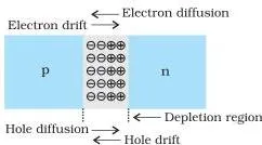
When the p and n regions are first formed, electrons diffuse from n to p and holes from p to n because of the concentration gradient (NCERT, p. 333). Each carrier that leaves exposes an immobile ionised core — positive donors on the n-side, negative acceptors on the p-side.
The result is the depletion region, a strip with no free charges, roughly one-tenth of a micrometre thick (NCERT, p. 333). The fixed charges set up an electric field that drives drift current, opposite in direction to the diffusion current. At equilibrium the two currents balance and no net current flows.
The potential that opposes further diffusion is the barrier potential \( V_0 \) (NCERT, p. 334).
The diode under bias
A diode is simply a p-n junction with metal contacts for applying an external voltage. Changing the barrier height with that voltage is the entire working of the device (NCERT, p. 334).
- Forward bias connects the p-side to the positive terminal. The applied voltage opposes \( V_0 \), so the effective barrier falls to \( (V_0 – V) \), the depletion layer narrows, and carriers cross in large numbers — minority carrier injection (NCERT, pp. 334–335). Current is in mA.
- Reverse bias connects the n-side to the positive terminal. The applied voltage adds to \( V_0 \), the barrier rises to \( (V_0 + V) \), and the depletion layer widens (NCERT, p. 336). Only a tiny drift current of minority carriers flows, in μA.
In forward bias the current stays negligible until the voltage crosses the threshold or cut-in voltage — about 0.7 V for silicon and 0.2 V for germanium — and then rises sharply (NCERT, p. 337).
In reverse bias the current is essentially voltage independent — the reverse saturation current — until the breakdown voltage \( V_{br} \), where it rises sharply. Beyond the manufacturer’s rated value the junction overheats and is destroyed (NCERT, p. 336).
The slope of the forward characteristic defines the dynamic resistance (NCERT, p. 337):
\[ r_d = \frac{\Delta V}{\Delta I} \quad (14.6) \]
Rectifiers: turning ac into dc
A diode conducts only when forward biased, which is exactly one half of each ac cycle. That one-way behaviour is what converts an alternating voltage into a unidirectional one — rectification (NCERT, p. 338).
- Half-wave rectifier: one diode in series with the load. Output appears only during the conducting half cycle (NCERT, p. 338).
- Full-wave rectifier: two diodes and a centre-tapped transformer. The two diodes conduct on alternate half cycles, so the output covers both halves (NCERT, p. 339).
- Capacitor filter: a capacitor across the load charges to the peak voltage and discharges through the load between peaks, smoothing the pulses. A large capacitance gives a large time constant \( CR \) and a slower fall (NCERT, pp. 339–340).
Use the chapter’s worked examples as checkpoints: 14.1 on why C, Si and Ge differ, 14.2 on doping numbers, 14.3 on junction formation, and 14.4 on reading a V-I curve.
Figure Walkthrough: Reading the Chapter’s Diagrams
The key diagrams of the chapter appear below, each explained so you can read it correctly in your book instead of glancing at it.
Energy band diagrams: what the bands and the gap mean
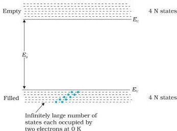
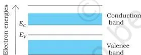
Fig 14.1 (NCERT, p. 326) shows a semiconductor at absolute zero: the valence band is completely filled and the conduction band is completely empty. \( E_C \) marks the bottom of the conduction band, \( E_V \) the top of the valence band, and the gap between them is \( E_g \).
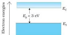
Fig 14.2 (NCERT, p. 326) compares the three cases. In a metal the bands overlap or the conduction band is partially filled, so electrons move freely. In an insulator the gap is over 3 eV and the conduction band stays empty. In a semiconductor the gap is 0.2 to 3 eV, and a few electrons cross it at room temperature.
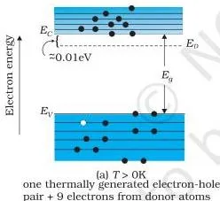
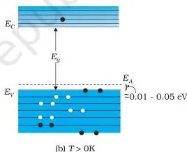
Fig 14.9 (NCERT, p. 332) shows what doping does to the bands. In n-type material the donor level \( E_D \) sits just below \( E_C \), so electrons jump into the conduction band with very little energy. In p-type material the acceptor level \( E_A \) sits just above \( E_V \), and valence electrons jump up into it, leaving holes behind.
Crystal pictures: covalent bonds and charge carriers
These are the atomic-level drawings that show where electrons and holes actually come from.
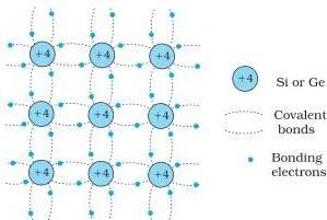
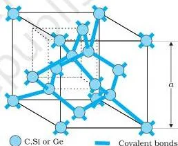
Fig 14.4 (NCERT, p. 328) is a two-dimensional drawing of the diamond-like structure. Each +4 core is a Si or Ge atom without its four valence electrons, and the shared pairs between cores are covalent bonds. At low temperature every bond is intact, so nothing conducts.
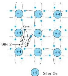
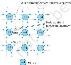
Fig 14.5 (NCERT, p. 328) shows the two results of thermal energy. In part (a) a broken bond produces a free electron and a hole at site 1. In part (b) an electron from site 2 fills that hole, so the hole appears to move from site 1 to site 2 — that apparent motion is the hole current.
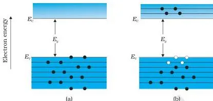
Fig 14.6 (NCERT, p. 329) says the same thing in band language. At T = 0 K the conduction band is empty and the intrinsic semiconductor behaves like an insulator. Above 0 K, thermally generated electron-hole pairs appear — filled circles are electrons, empty circles are holes.
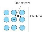
Fig 14.7 (NCERT, p. 330) introduces the pentavalent donor. Four of its electrons form the four bonds; the fifth is so weakly bound that room temperature frees it. The simplified picture beneath — a donor core with one extra positive charge and its electron — is the model to remember.
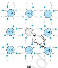
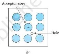
Fig 14.8 (NCERT, p. 331) does the same for a trivalent acceptor. One bond is simply missing — a hole — and the simplified picture is an acceptor core with one extra negative charge and its associated hole.
The junction and the diode under bias
These figures show how the junction forms and how an external voltage changes its behaviour.

Fig 14.10 (NCERT, p. 333) is the formation of the junction. Electrons and holes diffuse across, leaving immobile ionised donors on the n-side and acceptors on the p-side — the depletion region — and the field of those charges drives the drift current in the opposite direction.
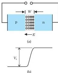
Fig 14.11 (NCERT, p. 334) shows the finished junction at equilibrium with no battery. The contact potential that has built up across the depletion region is the barrier potential \( V_0 \).
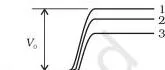
Fig 14.13 (NCERT, p. 335) shows forward bias. The battery opposes the built-in potential, and the three barrier diagrams — no battery, low voltage, high voltage — show the barrier shrinking until a large current flows.
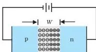
Fig 14.15 (NCERT, p. 336) shows reverse bias. The battery adds to the built-in potential, the barrier rises to \( (V_0 + V) \), and the depletion layer widens, so almost no current flows.
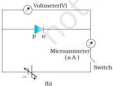
Fig 14.16 (NCERT, p. 336) is the V-I characteristic used for calculations. In forward bias a milliammeter is used because currents are large; the curve stays near zero until the threshold voltage, then rises almost vertically. In reverse bias a microammeter is used; the current stays flat at the reverse saturation value until breakdown.
Rectifier circuits: half-wave, full-wave and filtering
The last three diagrams show the diode doing its practical job of converting ac to dc.
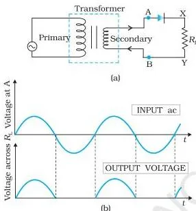
Fig 14.18 (NCERT, p. 338) is the half-wave rectifier. The diode conducts in the positive half cycle, so the output across the load is a series of half sinusoids — unidirectional but pulsing, with nothing during the negative half.
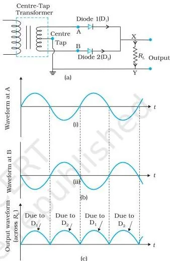
Fig 14.19 (NCERT, p. 339) is the full-wave rectifier. The secondary is centre-tapped, so diode D1 conducts when A is positive and D2 conducts when B is positive. Between them the two diodes cover both half cycles, and the output has no empty gaps.
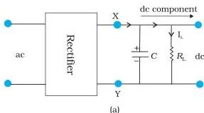
Fig 14.20 (NCERT, p. 340) adds the capacitor filter. The capacitor charges to the peak of each pulse and discharges slowly through the load between pulses, rounding off the valleys. The much smoother output is what a power supply needs.
Key Terms and Definitions: A Semiconductor Electronics Glossary
Quick, plain definitions of the terms the chapter uses, with the textbook page where each one appears.
| Term | Plain definition | NCERT page |
|---|---|---|
| Semiconductor | A solid whose resistivity lies between metals and insulators, \( 10^{-5} \) to \( 10^{6}\ \Omega\ \text{m} \) | 324 |
| Hole | An electron vacancy in a covalent bond that behaves as an apparent particle with effective charge \( +q \) | 327 |
| Intrinsic semiconductor | A pure semiconductor whose carriers come only from thermal generation, so \( n_e = n_h = n_i \) | 327 |
| Doping | Deliberately adding a few ppm of a suitable impurity to raise conductivity | 329 |
| Dopant | The impurity atom added during doping | 329 |
| Donor | A pentavalent impurity (P, As, Sb) that contributes an extra conduction electron | 330 |
| Acceptor | A trivalent impurity (B, Al, In) that creates a hole for conduction | 331 |
| n-type semiconductor | Doped Si or Ge in which electrons are majority carriers, \( n_e \gg n_h \) | 331 |
| p-type semiconductor | Doped Si or Ge in which holes are majority carriers, \( n_h \gg n_e \) | 331 |
| Depletion region | The layer of immobile ionised donors and acceptors around the junction, about \( 0.1\ \mu\text{m} \) thick, with no free charges | 333 |
| Barrier potential | The junction potential \( V_0 \) that opposes further diffusion of carriers at equilibrium | 334 |
| Forward bias | p-side to positive, n-side to negative; the effective barrier becomes \( (V_0 – V) \) | 334 |
| Reverse bias | n-side to positive, p-side to negative; the effective barrier becomes \( (V_0 + V) \) | 335 |
| Threshold (cut-in) voltage | The forward voltage beyond which diode current rises sharply; about 0.7 V for Si, 0.2 V for Ge | 337 |
| Reverse saturation current | The small, nearly voltage-independent reverse current of minority carriers, in μA | 337 |
| Breakdown voltage | The reverse voltage \( V_{br} \) at which reverse current rises sharply; beyond the rated value the diode overheats and is destroyed | 336 |
| Dynamic resistance | The ratio of a small change in diode voltage to the small change in current, \( r_d = \Delta V / \Delta I \) | 337 |
| Rectifier | A circuit that converts an alternating voltage into a unidirectional, pulsating output using a diode | 338 |
| Filter | A capacitor or inductor arrangement that smooths the rectified output toward steady dc | 339 |
Common Mistakes Students Make in Semiconductor Electronics
Six ideas in this chapter trip up most students, and the textbook itself flags several of them in its Points to Ponder (NCERT, p. 341). The table names each mistake before you make it.
| Mistake | Correct rule | How to check your answer |
|---|---|---|
| Treating \( E_C \) and \( E_V \) as lines at fixed spots inside the crystal | They are delocalised averages — the drawn lines only mark the bottom of the conduction band and the top of the valence band | If your answer treats the bands as being at a particular place, rewrite it as an average over the whole solid (Points to Ponder 1, NCERT, p. 341) |
| Calling a hole a real particle | A hole is a bond vacancy with effective charge \( +q \); its motion describes bound electrons shifting between bonds | Trace the electron that fills the hole — the vacancy left behind is the hole (NCERT, p. 327) |
| Mixing up the dopants | Pentavalent donors (P, As, Sb) make n-type; trivalent acceptors (B, Al, In) make p-type | Check the dopant’s group in the periodic table — group 15 donates, group 13 accepts |
| Believing a doped crystal carries net charge | Extrinsic semiconductors keep overall charge neutrality — added carriers are balanced by ionised cores | Count charges: every extra electron matches a +1 ionised donor (Summary point 9, NCERT, p. 341) |
| Expecting reverse current to grow with voltage | Reverse saturation current is essentially voltage independent until \( V_{br} \); past the rated value the junction overheats and is destroyed | Read the reverse leg of the V-I curve — flat at μA, then a vertical jump at breakdown (NCERT, p. 336) |
| Forgetting the rectifier frequency rule | Half-wave output frequency equals the input frequency; full-wave output is double it | 50 Hz input gives 50 Hz half-wave and 100 Hz full-wave (Exercise 14.6) |
One more caution from the chapter: a p-n junction cannot be made by physically joining two slabs, because no slab is flat at the atomic scale (Example 14.3, NCERT, p. 334).
Exam Notes: What the Exercises Test and the Calculations to Practise
The chapter’s exercises test concept recall more than calculation, but two calculations recur in the worked examples. This section maps the six end-of-chapter exercises and gives original numbers to practise on.
What each exercise asks:
| Exercise | Concept tested | What a full answer needs |
|---|---|---|
| 14.1 | n-type carriers and dopants | Electrons are majority carriers, holes minority, and the dopants are pentavalent — option (c) |
| 14.2 | The p-type counterpart of 14.1 | Holes are majority carriers, electrons minority, and the dopants are trivalent — option (d) |
| 14.3 | Band gap ordering of C, Si and Ge | \( (E_g)_C \gt (E_g)_{Si} \gt (E_g)_{Ge} \) — option (c), matching 5.4, 1.1 and 0.7 eV |
| 14.4 | Why holes diffuse from p to n in an unbiased junction | Because the hole concentration is higher in the p-region — a concentration gradient — option (c) |
| 14.5 | Effect of forward bias | It lowers the potential barrier — option (c) |
| 14.6 | Rectifier output frequency | 50 Hz from a half-wave rectifier, 100 Hz from a full-wave rectifier, for a 50 Hz input |
Worked example — dynamic resistance from a V-I characteristic. A silicon diode’s forward characteristic reads \( I = 15\ \text{mA} \) at \( V = 0.78\ \text{V} \) and \( I = 25\ \text{mA} \) at \( V = 0.85\ \text{V} \). Find the dynamic resistance.
Step 1: Read the small changes.
\( \Delta V = 0.85 – 0.78 = 0.07\ \text{V} \) and \( \Delta I = 25 – 15 = 10\ \text{mA} = 0.010\ \text{A} \).
\[ r_d = \frac{\Delta V}{\Delta I} = \frac{0.07\ \text{V}}{0.010\ \text{A}} = 7\ \Omega \]
Final answer: \( r_d = 7\ \Omega \). Use the change in V divided by the change in I, not the total values.
Now the reverse-bias contrast: at \( V = -8\ \text{V} \) the diode current is \( -0.8\ \mu\text{A} \). What resistance does it offer?
\[ R = \frac{8\ \text{V}}{0.8\ \mu\text{A}} = \frac{8}{8 \times 10^{-7}} = 10^{7}\ \Omega \]
Compare the two results: forward resistance of a few ohms, reverse resistance of ten megohms. That ten-million-fold difference is why the diode acts as a one-way switch.
Rules to remember: with a 50 Hz input, half-wave output is 50 Hz and full-wave output is 100 Hz (Exercise 14.6). Also note the Points to Ponder 2 edge case (NCERT, p. 341): in compound semiconductors the type can change with the ratio of elements — gallium-rich GaAs is \( Ga_{1.1}As_{0.9} \), arsenic-rich GaAs is \( Ga_{0.9}As_{1.1} \).
Textbook contents and the examinable syllabus are not always identical — check the current official Class 12 Physics syllabus on the CBSE website before deciding what to revise.
Revision Summary: The Whole Chapter in One Page
This list rewrites the chapter’s own Summary (NCERT, pp. 340–341) for a last-minute read. Skim it twice and you have the chapter:
- Solids are classified by resistivity: metals \( 10^{-2} \)–\( 10^{-8} \), semiconductors \( 10^{-5} \)–\( 10^{6} \), insulators \( 10^{11} \)–\( 10^{19}\ \Omega\ \text{m} \) (NCERT, p. 324).
- Conduction depends on the energy gap \( E_g \) between the valence and conduction bands (NCERT, p. 325).
- Metals have \( E_g \approx 0 \), insulators \( E_g \gt 3\ \text{eV} \), semiconductors 0.2 to 3 eV (NCERT, p. 341).
- Gap values: C 5.4 eV, Si 1.1 eV, Ge 0.7 eV, Sn 0 eV (NCERT, p. 332).
- An intrinsic semiconductor has equal electrons and holes: \( n_e = n_h = n_i \) (NCERT, p. 327).
- A hole is an electron vacancy with effective charge \( +q \); total current is \( I = I_e + I_h \) (NCERT, pp. 327–328).
- Doping — a few ppm of impurity — multiplies conductivity (NCERT, p. 329).
- Pentavalent donors (P, As, Sb) give n-type with \( n_e \gg n_h \) (NCERT, p. 331).
- Trivalent acceptors (B, Al, In) give p-type with \( n_h \gg n_e \) (NCERT, p. 331).
- Mass action law: \( n_e n_h = n_i^2 \); the crystal always stays electrically neutral (NCERT, pp. 332, 341).
- The p-n junction has a depletion layer of immobile ions, about \( 0.1\ \mu\text{m} \) thick, and a barrier potential (NCERT, pp. 333–334).
- Forward bias lowers the barrier to \( (V_0 – V) \); reverse bias raises it to \( (V_0 + V) \) (NCERT, pp. 334–336).
- Forward current is in mA, reverse saturation current in μA; threshold about 0.7 V for Si, 0.2 V for Ge (NCERT, p. 337).
- Diodes rectify ac; a capacitor filter smooths the pulses toward dc (NCERT, pp. 338–340).
The three semiconductor types side by side:
| Intrinsic | n-type | p-type | |
|---|---|---|---|
| Dopant | None — pure crystal | Pentavalent: P, As, Sb | Trivalent: B, Al, In |
| Carrier relation | \( n_e = n_h = n_i \) | \( n_e \gg n_h \) | \( n_h \gg n_e \) |
| Majority carriers | Electrons and holes equally | Electrons | Holes |
| Minority carriers | — | Holes | Electrons |
| Dopant energy level | — | Donor level \( E_D \) just below \( E_C \) | Acceptor level \( E_A \) just above \( E_V \) |
Related Resources
If you came for the book itself, this chapter sits in the NCERT Class 12 Physics book page, inside the Class 12 hub; the NCERT books home page covers every class from 6 to 12.
For revision, the notes that pair with this chapter:
- Class 12 Physics notes — topic-wise explanations for the whole book
- Alternating Current Class 12 notes — the chapter that explains the ac input this chapter’s rectifiers convert
- Nuclei Class 12 notes — the chapter that follows this one in the book
- Class 12 study resources — notes for every subject
- NCERT notes home — notes from Class 6 to Class 12
Reference: NCERT Class 12 Physics textbook, Semiconductor Electronics: Materials, Devices and Simple Circuits chapter, official edition on ncert.nic.in.
Sources and Data Verification
- Editions described: the section titles, page numbers, figure captions and exercise references on this page come from the NCERT Class 12 Physics Part II textbook, Chapter 14, “Semiconductor Electronics: Materials, Devices and Simple Circuits”, 2026-27 reprint, official PDF from ncert.nic.in.
- What this page covers: the contents table and page references describe only this NCERT textbook chapter; they are not the complete CBSE scheme for Class 12.
- Academic session: this page is maintained for the 2026-27 session.
- Which authority settles what: NCERT publishes the textbooks, editions and official PDFs; CBSE sets the curriculum, syllabus and examinations.
Semiconductor Electronics: Class 12 Frequently Asked Questions
Why does a p-n junction diode allow current in only one direction?
In forward bias the applied voltage opposes the barrier potential, lowering it from \( V_0 \) to \( (V_0 – V) \), so carriers cross easily. In reverse bias the barrier rises to \( (V_0 + V) \), so only a tiny drift current of minority carriers flows (NCERT, pp. 334–336). The diode therefore conducts strongly one way and almost not at all the other.
What is the difference between n-type and p-type semiconductors?
n-type is made by doping with pentavalent donors (P, As, Sb), so electrons are the majority carriers and \( n_e \gg n_h \); the donor level sits just below the conduction band.
p-type is made with trivalent acceptors (B, Al, In), so holes are the majority carriers and \( n_h \gg n_e \); the acceptor level sits just above the valence band (NCERT, pp. 330–332).
What happens to the depletion layer in forward bias and reverse bias?
Forward bias narrows the depletion layer; reverse bias widens it (NCERT, pp. 335–336). The applied voltage either opposes the junction field, letting carriers close in from both sides, or adds to it, pushing the immobile ionised cores further apart.
What is the output frequency of a half-wave and a full-wave rectifier for a 50 Hz input?
50 Hz for the half-wave rectifier and 100 Hz for the full-wave rectifier (Exercise 14.6). The half-wave output repeats once per input cycle; the full-wave output produces a pulse in each half cycle, so it repeats twice per cycle.
What are the threshold voltages of silicon and germanium diodes?
About 0.7 V for silicon and 0.2 V for germanium (NCERT, p. 337). Below the threshold the forward current is negligible; above it, the current rises sharply.
Are doped semiconductors electrically neutral?
Yes. The charge of the added carriers is exactly balanced by the ionised cores of the dopant atoms, so the crystal always maintains overall charge neutrality (NCERT, p. 341). This holds for both n-type and p-type materials.
Reference: NCERT Class 12 Physics textbook, chapter 14, official edition on ncert.nic.in.
Explore Class 12 Physics Books
Class 12 Physics on LearnCBSE:
Related chapters: