This sheet gathers the semiconductor electronics class 12 formulas from NCERT Chapter 14 that you revise most: carrier concentrations in intrinsic and doped semiconductors, the mass action law, diode dynamic resistance, junction barrier heights under bias, and rectifier output frequencies. It also covers the resistivity-conductivity ranges and energy-gap criteria used to classify metals, semiconductors and insulators.
Each formula is grouped by topic, followed by a symbol table, when-to-use guidance, worked examples with original numbers, and chapter-specific common mistakes. For the derivations and the full band-theory discussion, open the chapter’s official NCERT Physics Part II PDF; for the rest of your syllabus, browse the Class 12 formulas index.
Formulas at a Glance
Quick index of every formula on this page. Symbol meanings are in the next section; the conditions attached to each formula are in the when-to-use table.
| Purpose (what you are finding) | Formula |
|---|---|
| Resistivity from conductivity (or the reverse) | \( \rho = \dfrac{1}{\sigma} \) |
| Carrier densities in a pure (intrinsic) semiconductor | \( n_e = n_h = n_i \) |
| Total current carried by electrons and holes together | \( I = I_e + I_h \) |
| n-type: electrons are the majority carriers | \( n_e \gg n_h \) |
| p-type: holes are the majority carriers | \( n_h \gg n_e \) |
| Mass action law: product of carrier densities in thermal equilibrium | \( n_e n_h = n_i^2 \) |
| Electron density of a heavily doped n-type sample (from the doping concentration) | \( n_e \approx N_D \) |
| Effective barrier height under forward bias | \( V_0 – V \) |
| Effective barrier height under reverse bias | \( V_0 + V \) |
| Dynamic resistance of a diode at an operating point | \( r_d = \dfrac{\Delta V}{\Delta I} \) |
| Half-wave rectifier output frequency (derived from the rectifier action) | \( f_{out} = f_{in} \) |
| Full-wave rectifier output frequency (derived from the rectifier action) | \( f_{out} = 2 f_{in} \) |
| Time constant of the capacitor filter | \( \tau = R_L C \) |
All Formulas, Grouped by Topic
The formulas below follow the order of the textbook sections, with the NCERT equation number where the chapter numbers one.
Classification by Conductivity and Energy Gap
Resistivity and conductivity are reciprocals, and the chapter classifies solids by the order of magnitude of either. (NCERT, p. 324) \[ \rho = \frac{1}{\sigma} \]
Indicative room-temperature ranges (NCERT, p. 324):
| Material | Resistivity \( \rho \) (\( \Omega\,\text{m} \)) | Conductivity \( \sigma \) (S m⁻¹) |
|---|---|---|
| Metals | \( 10^{-2} \) to \( 10^{-8} \) | \( 10^{2} \) to \( 10^{8} \) |
| Semiconductors | \( 10^{-5} \) to \( 10^{6} \) | \( 10^{5} \) to \( 10^{-6} \) |
| Insulators | \( 10^{11} \) to \( 10^{19} \) | \( 10^{-11} \) to \( 10^{-19} \) |
Conductivity can also be judged from the energy band gap \( E_g \): insulators have \( E_g \gt 3 \) eV, semiconductors have \( E_g \) between 0.2 eV and 3 eV, and metals have \( E_g \approx 0 \). (NCERT, p. 341) Specific values for the group-IV elements: C (diamond) 5.4 eV, Si 1.1 eV, Ge 0.7 eV and Sn 0 eV.
This is why diamond is an insulator, Si and Ge are semiconductors, and Sn is a metal. (NCERT, p. 332)
Intrinsic Semiconductors
In a pure (intrinsic) semiconductor, every thermally broken covalent bond creates one free electron and one hole, so the two densities are exactly equal. (NCERT, p. 327) \[ n_e = n_h = n_i \quad (14.1) \]
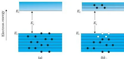
The figure contrasts the two situations: at \( T = 0 \) K the conduction band is empty, while above 0 K equal numbers of electrons and holes appear. That equality is the physical content of \( n_e = n_h = n_i \).
Under an applied electric field, both carriers contribute to the total current. (NCERT, p. 328) \[ I = I_e + I_h \quad (14.2) \]
Extrinsic Semiconductors: n-type and p-type
Doping adds one carrier type in large numbers. A pentavalent donor (As, Sb, P) contributes a fifth, weakly bound electron, so electrons become the majority carriers and the sample is n-type. (NCERT, p. 330) \[ n_e \gg n_h \quad \text{(n-type)} \quad (14.3) \]
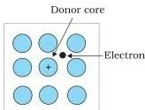
As the picture shows, four of the donor’s electrons form bonds with the four silicon neighbours; the fifth is free to move at room temperature. Only about \( 0.01 \) eV (Ge) or \( 0.05 \) eV (Si) is needed to free it, far less than the forbidden gap of about \( 0.72 \) eV (Ge) or \( 1.1 \) eV (Si).
(NCERT, p. 330) A trivalent acceptor (B, Al, In) has one valence electron fewer than Si or Ge; the missing bond behaves as a hole, making holes the majority carriers of a p-type sample. (NCERT, p. 331) \[ n_h \gg n_e \quad \text{(p-type)} \quad (14.4) \]
In thermal equilibrium, the product of the two carrier densities in any doped sample equals the square of the intrinsic concentration. (NCERT, p. 332) This is the mass action law, the most-used working formula of the chapter.
\[ n_e n_h = n_i^2 \quad (14.5) \]
For a heavily doped n-type sample, the electron density is set by the donor concentration itself:
\[ n_e \approx N_D \]
This is valid only when \( N_D \gg n_i \). The minority-hole density then follows from the mass action law: \( n_h = n_i^2 / n_e \).
p-n Junction: Barrier Heights
At equilibrium a barrier potential \( V_0 \) develops across the junction because diffusion leaves immobile ionised donors on the n-side and ionised acceptors on the p-side. (NCERT, p. 334) The depletion region that forms is about one-tenth of a micrometre thick. (NCERT, p. 333) An external voltage \( V \) changes the barrier.
Forward bias (p-side to the positive terminal) opposes \( V_0 \), so the effective barrier falls. (NCERT, p. 334) \[ \text{barrier (forward bias)} = V_0 – V \]
Reverse bias (n-side to the positive terminal) adds to \( V_0 \), raising the barrier and suppressing diffusion current. (NCERT, p. 335) \[ \text{barrier (reverse bias)} = V_0 + V \]
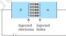
As the figure shows, increasing the forward voltage shrinks the barrier from \( V_0 \) towards zero; conduction becomes significant once the applied voltage approaches \( V_0 \).
Diode Characteristics
A diode has no single fixed resistance. Its dynamic resistance is the slope of the V-I curve at an operating point. (NCERT, p. 336) \[ r_d = \frac{\Delta V}{\Delta I} \quad (14.6) \]
Two characteristic voltages worth memorising (NCERT, p. 336):
- Threshold (cut-in) voltage – about 0.2 V for a germanium diode and 0.7 V for a silicon diode; current rises steeply only beyond this voltage.
- Breakdown voltage \( V_{br} \) – in reverse bias the current stays at a tiny microampere reverse saturation level up to \( V_{br} \), then rises sharply. Without an external current limit, the junction overheats and is destroyed.
Rectifiers
Because a diode conducts only when forward biased, it converts ac into a unidirectional pulsating output. A half-wave rectifier conducts during one half of each input cycle, so the output has one pulse per input cycle. (NCERT, p. 338) \[ f_{out} = f_{in} \quad \text{(half-wave)} \]
A full-wave rectifier (two diodes with a centre-tapped transformer) conducts during both half-cycles, giving two output pulses per input cycle. (NCERT, pp. 338-339) \[ f_{out} = 2 f_{in} \quad \text{(full-wave)} \]
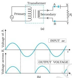
Part (c) shows why the frequency doubles: a pulse arrives every half-cycle, so there are two output pulses for every input cycle.
To smooth the pulses, a capacitor filter is connected across the load. The capacitor discharges through \( R_L \) with a time constant, so the output falls slowly between pulses. (NCERT, p. 339) \[ \tau = R_L C \]
A large \( C \) gives a long time constant, so the voltage falls less between pulses and the output stays close to the peak rectified voltage.
What Each Symbol Means
Units are SI; energy levels are quoted in electronvolts, the unit the chapter uses for band diagrams.
| Symbol | What it means | Unit |
|---|---|---|
| \( \rho \) | Resistivity of the material | \( \Omega\,\text{m} \) (ohm metre) |
| \( \sigma \) | Conductivity of the material | \( \text{S m}^{-1} \) (siemens per metre) |
| \( n_e \) | Number density of conduction (free) electrons | \( \text{m}^{-3} \) |
| \( n_h \) | Number density of holes | \( \text{m}^{-3} \) |
| \( n_i \) | Intrinsic carrier concentration of the pure semiconductor | \( \text{m}^{-3} \) |
| \( N_D \) | Concentration of donor atoms in a doped sample | \( \text{m}^{-3} \) |
| \( I \) | Total current through the semiconductor | A (ampere) |
| \( I_e \) | Electron current | A (ampere) |
| \( I_h \) | Hole current | A (ampere) |
| \( E_g \) | Energy band gap between the valence and conduction bands | eV (electronvolt) |
| \( E_C \) | Energy at the bottom of the conduction band | eV (electronvolt) |
| \( E_V \) | Energy at the top of the valence band | eV (electronvolt) |
| \( V_0 \) | Barrier (built-in) potential of the junction | V (volt) |
| \( V \) | Externally applied voltage across the diode | V (volt) |
| \( V_{br} \) | Breakdown voltage: reverse voltage at which current rises sharply | V (volt) |
| \( r_d \) | Dynamic resistance of the diode | \( \Omega \) (ohm) |
| \( \Delta V \) | Small change in diode voltage | V (volt) |
| \( \Delta I \) | Small change in diode current | A (ampere) |
| \( f_{in} \) | Input ac frequency | Hz (hertz) |
| \( f_{out} \) | Rectified output frequency | Hz (hertz) |
| \( R_L \) | Load resistance | \( \Omega \) (ohm) |
| \( C \) | Filter capacitance | F (farad) |
| \( \tau \) | Time constant of the R-C filter | s (second) |
When to Use Each Formula
| Formula | Use it when … | Condition to check |
|---|---|---|
| \( \rho = 1/\sigma \) | Converting between resistivity and conductivity, or comparing materials by their ranges. | The ranges are order-of-magnitude indicators only. |
| \( n_e = n_h = n_i \) | The sample is pure (intrinsic) Si or Ge and you need the mobile carrier density. | No doping; thermal equilibrium. |
| \( I = I_e + I_h \) | An electric field acts on a semiconductor and both carrier types move. | Both electrons and holes are present. |
| \( n_e \gg n_h \) | Identifying n-type material from its carriers. | Doped with a pentavalent donor (As, Sb, P). |
| \( n_h \gg n_e \) | Identifying p-type material from its carriers. | Doped with a trivalent acceptor (B, Al, In). |
| \( n_e n_h = n_i^2 \) | Finding the minority density when the majority density is known. | Thermal equilibrium. |
| \( n_e \approx N_D \) | Estimating the majority electron density of a doped n-type sample. | \( N_D \gg n_i \), i.e. much larger than about \( 1.5 \times 10^{16}\ \text{m}^{-3} \) for Si. |
| \( V_0 – V \) | Effective barrier height under forward bias. | p-side connected to the positive terminal. |
| \( V_0 + V \) | Effective barrier height under reverse bias. | n-side connected to the positive terminal. |
| \( r_d = \Delta V/\Delta I \) | Small-signal resistance at a point on the diode’s V-I curve. | Small changes about one operating point. |
| \( f_{out} = f_{in} \) | Output frequency of a half-wave rectifier. | One conducting half-cycle per input cycle. |
| \( f_{out} = 2 f_{in} \) | Output frequency of a full-wave rectifier. | Both half-cycles conduct. |
| \( \tau = R_L C \) | Judging how fast the capacitor-filter output falls between pulses. | Large \( C \) gives a steadier dc output. |
Worked Examples
Three examples with original numbers so you can practise the working, not just read it. For formulas from other chapters and classes, browse the physics formula sheet collection.
Worked Example 1: Carrier Densities in Arsenic-Doped Silicon
Step 1: Decide the type.
Arsenic is pentavalent, so it is a donor: the sample is n-type and \( n_e \gg n_h \).
- Step 1: Since \( N_D = 2 \times 10^{21}\ \text{m}^{-3} \) is far larger than \( n_i = 1.5 \times 10^{16}\ \text{m}^{-3} \), use the approximation \[ n_e \approx N_D = 2 \times 10^{21}\ \text{m}^{-3} \]
- Step 2: Find the hole density from the mass action law, \( n_e n_h = n_i^2 \):
\[ n_h = \frac{n_i^2}{n_e} = \frac{(1.5 \times 10^{16})^2}{2 \times 10^{21}} = \frac{2.25 \times 10^{32}}{2 \times 10^{21}} \approx 1.1 \times 10^{11}\ \text{m}^{-3} \]
Final answer: \( n_e \approx 2 \times 10^{21}\ \text{m}^{-3} \) (electrons, majority) and \( n_h \approx 1.1 \times 10^{11}\ \text{m}^{-3} \) (holes, minority). Quick check: the product \( n_e n_h = 2.25 \times 10^{32}\ \text{m}^{-6} = n_i^2 \), as required.
Worked Example 2: Dynamic Resistance from the V-I Curve
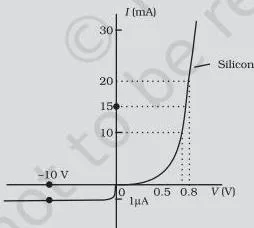
The dynamic resistance is read from a curve such as this one by taking the slope at the operating point.
- Step 1: Write the formula for the slope of the V-I curve: \( r_d = \Delta V/\Delta I \).
- Step 2: Read two nearby points: \( I_1 = 8\ \text{mA} \) at \( V_1 = 0.71\ \text{V} \) and \( I_2 = 18\ \text{mA} \) at \( V_2 = 0.79\ \text{V} \).
Convert the current change to amperes before dividing.
\[ \Delta V = 0.79 – 0.71 = 0.08\ \text{V}, \qquad \Delta I = 18 – 8 = 10\ \text{mA} = 0.010\ \text{A} \]
\[ r_d = \frac{\Delta V}{\Delta I} = \frac{0.08\ \text{V}}{0.010\ \text{A}} = 8\ \Omega \]
Final answer: \( r_d = 8\ \Omega \) at this operating point. The same diode reverse biased at \( V = -11\ \text{V} \) shows \( I = -1\ \mu\text{A} \), giving \( 11\ \text{V} / 1\ \mu\text{A} = 1.1 \times 10^{7}\ \Omega \) — the forward-reverse contrast in one number.
Worked Example 3: Output Frequency of Half-Wave and Full-Wave Rectifiers
Step 1: Count output pulses per input cycle.
Half-wave conducts in one half-cycle only, so one pulse per cycle gives \( f_{out} = f_{in} \).
Full-wave conducts in both half-cycles, so two pulses per cycle gives \( f_{out} = 2 f_{in} \).
Step 2: Substitute \( f_{in} = 60\ \text{Hz} \):
\[ \text{half-wave: } f_{out} = 60\ \text{Hz}; \qquad \text{full-wave: } f_{out} = 2 \times 60\ \text{Hz} = 120\ \text{Hz} \]
Final answer: 60 Hz for the half-wave rectifier and 120 Hz for the full-wave rectifier on the same 60 Hz input.
Common Mistakes to Avoid
Each row gives the error, the rule that fixes it, and a check you can run on your own answer.
| Mistake | Correct rule | How to check your answer |
|---|---|---|
| Writing the mass action law as \( n_e n_h = n_i \) (the square dropped) | In thermal equilibrium, \( n_e n_h = n_i^2 \). | Multiply your two densities: for Si at room temperature the product must be \( 2.25 \times 10^{32}\ \text{m}^{-6} \) when \( n_i = 1.5 \times 10^{16}\ \text{m}^{-3} \). |
| Saying electrons are the minority carriers in n-type silicon (or holes in p-type) | Pentavalent donor gives electrons as majority carriers in n-type; trivalent acceptor gives holes as majority carriers in p-type. | Check the dopant’s valency: 5 gives \( n_e \gg n_h \), 3 gives \( n_h \gg n_e \). |
| Using \( V_0 + V \) for the forward-bias barrier | Forward bias opposes \( V_0 \), so the barrier is \( V_0 – V \); reverse bias adds to it, giving \( V_0 + V \). | Forward current is of the order of mA — that happens only when the barrier has been lowered. |
| Leaving \( \Delta I \) in mA inside \( r_d = \Delta V/\Delta I \) | Convert the current change to amperes first: \( 10\ \text{mA} = 0.010\ \text{A} \). | A forward \( r_d \) of order \( 10^{3}\ \Omega \) or more means you divided volts by milliamps; expect single-digit to tens of ohms. |
| Taking the full-wave output frequency as equal to the input frequency | Full-wave doubles the pulse rate: \( f_{out} = 2 f_{in} \). | Count the output pulses in one input cycle: two for full-wave, one for half-wave. |
Frequently Asked Questions
Why are \( n_e \) and \( n_h \) equal in an intrinsic semiconductor but not in a doped one?
In a pure crystal, every thermally broken covalent bond creates exactly one free electron and one hole, so the counts stay equal. Doping breaks the balance: a pentavalent donor adds an electron without a hole, while a trivalent acceptor adds a hole without an electron.
When exactly can I use \( n_e \approx N_D \)?
Only when the donor concentration is much larger than the intrinsic concentration \( n_i \) (about \( 1.5 \times 10^{16}\ \text{m}^{-3} \) for Si at room temperature). If the doping is weak, thermal generation contributes noticeably and you must use the full mass action relation \( n_e n_h = n_i^2 \) instead.
Why is a diode’s reverse current so small and nearly constant?
Reverse current is drift current: minority carriers are swept across the junction by the electric field. Their supply is limited by thermal generation, not by the applied voltage, so raising the reverse voltage barely changes the current — until the breakdown voltage \( V_{br} \), where the current rises sharply and can destroy the diode if it is not limited externally.
What does dynamic resistance tell me that ordinary resistance does not?
A diode has no single V/I value because its V-I curve is not a straight line. \( r_d = \Delta V/\Delta I \) measures the local slope at an operating point — how much the voltage moves for a small current change. That is the quantity you need when the diode carries a small signal on top of a steady current.
Reference: NCERT Class 12 Physics textbook, chapter Semiconductor Electronics: Materials, Devices and Simple Circuits.
Explore Class 12 Physics Formulas
More for this chapter:
Class 12 Physics on LearnCBSE:
Related chapters: