
These semiconductor electronics class 12 physics notes compress Chapter 14 of the NCERT textbook into what you actually need before a test: energy bands, intrinsic and extrinsic semiconductors, the p-n junction, diode biasing and rectifiers — plus the formulas, worked examples and exam pointers that carry marks. They are part of the Class 12 Physics notes collection on this site.
Read the sections top to bottom the first time to build the ideas in order. For last-night revision, jump straight to the Formula Box, the two worked examples and the common-mistakes table. Every key term is bolded on first use, and NCERT page numbers are cited so you can cross-check any idea against the official textbook at ncert.nic.in.
Chapter Map: From Vacuum Valves to the p-n Junction
Before 1948, electronics ran on vacuum tubes (valves): a heated cathode supplied electrons that flowed through an evacuated space between electrodes. These devices were bulky, consumed high power, operated at high voltages (around 100 V) and had short life and low reliability (NCERT, p. 1).
Solid-state semiconductor devices replaced them because the charge carriers move within the solid itself — no heated cathode, no vacuum. They are small, consume low power, run at low voltages and last far longer. Simple excitations like light, heat or a small applied voltage change the number of mobile charges a semiconductor carries.
The chapter builds one idea on the next. Learn it in this order:
- Conductivity classification and energy bands — how solids are sorted into metals, insulators and semiconductors.
- Intrinsic semiconductors — pure material with equal numbers of electrons and holes.
- Doping and extrinsic semiconductors — n-type and p-type.
- The p-n junction — diffusion, drift and the depletion region.
- Diode behaviour under bias — how the barrier changes and the V-I curve.
- The diode as a rectifier — turning ac into dc.
As NCERT’s summary stresses, the p-n junction is the “key” to all semiconductor devices (NCERT, p. 18, summary point 12) — a junction diode, a transistor and an integrated circuit all start from it.
Classification of Solids: Conductivity Ranges and Energy Bands
Solids are sorted two independent ways: by resistivity and by energy band structure. Both give the same three families — metals, semiconductors and insulators. The resistivity ranges below are indicative of magnitude, not exact limits (NCERT, p. 2).
| Type | Resistivity \( \rho \) (Ω m) | Conductivity \( \sigma \) (S m⁻¹) |
|---|---|---|
| Metals | \(10^{-2}\) to \(10^{-8}\) | \(10^2\) to \(10^{8}\) |
| Semiconductors | \(10^{-5}\) to \(10^{6}\) | \(10^{5}\) to \(10^{-6}\) |
| Insulators | \(10^{11}\) to \(10^{19}\) | \(10^{-11}\) to \(10^{-19}\) |
When atoms form a solid, the outer electron orbits of neighbours come close or overlap, so each electron sees a slightly different charge pattern and sits at a slightly different energy level. These closely spaced levels form energy bands. The band holding the valence electrons is the valence band; the band above it is the conduction band.
The gap between the top of the valence band and the bottom of the conduction band is the energy band gap \(E_g\) (NCERT, p. 4). Its size decides the material’s behaviour:
- Metals (\(E_g \approx 0\)): the conduction band is partially filled or overlaps the valence band, so electrons move freely — low resistance, high conductivity.
- Insulators (\(E_g \gt 3\) eV): the conduction band is empty and thermal excitation cannot push electrons across the huge gap — no conduction.
- Semiconductors (\(E_g \lt 3\) eV): at room temperature some valence electrons gain enough energy to cross the gap, giving measurable but small conduction (NCERT, p. 4; p. 19, summary point 11).
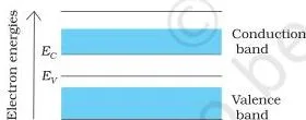
Figure 14.2(a) shows Case I, the metal: the conduction band is partially filled or the two bands overlap, so a large number of electrons are free for conduction.
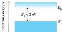
Figure 14.2(b) shows Case II, the insulator: a large gap \(E_g \gt 3\) eV with no electrons in the conduction band, so no conduction is possible. The semiconductor case sits in between — a small gap \(E_g \lt 3\) eV.
Memorise these gap values — they appear repeatedly in exams:
| Element (group IV) | Energy band gap |
|---|---|
| Carbon C (diamond) | 5.4 eV (insulator) |
| Silicon Si | 1.1 eV (semiconductor) |
| Germanium Ge | 0.7 eV (semiconductor) |
| Tin Sn | 0 eV (metallic) |
The gap falls from carbon to germanium, which is why Si and Ge are semiconductors while carbon is an insulator; tin ends the list as a metal because its gap is zero (NCERT, p. 10).
Intrinsic Semiconductors: Covalent Bonds, Holes and Carrier Balance
An intrinsic semiconductor is a pure semiconductor such as Si or Ge. Its atoms sit in a diamond-like lattice, each surrounded by four nearest neighbours (NCERT, p. 5). Every Si or Ge atom shares its four valence electrons with four neighbours, and these shared electron pairs form covalent bonds.
At low temperatures all bonds are intact and no free carriers exist. When thermal energy breaks a bond, the electron that frees itself (charge −q) moves into the lattice as a conduction electron, while the bond it left holds a vacancy with effective positive charge +q.
That vacancy is a hole — NCERT calls it “an apparent free particle” with effective positive charge. It is a useful description, not a real particle (NCERT, p. 5).
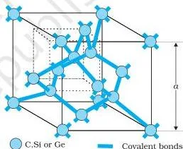
As Fig 14.5 shows, a hole “moves” because a bound electron from a neighbouring bond jumps into the vacancy, shifting the vacancy to that bond. The original free electron moves independently and gives the electron current \(I_e\); holes give the hole current \(I_h\). Total current: \(I = I_e + I_h\) (14.2) (NCERT, p. 6).
In a pure crystal electrons and holes are created in equal numbers, because every broken bond yields one of each:
\[ n_e = n_h = n_i \quad (14.1) \]
Here \(n_i\) is the intrinsic carrier concentration. Generation is balanced by recombination — a free electron colliding with and filling a hole. At equilibrium the rates of the two processes are equal (NCERT, p. 6).
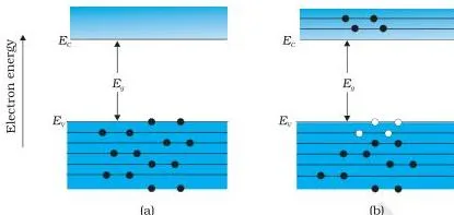
The diagram above makes this concrete: at \(T = 0\) K the conduction band is empty, so the material behaves like an insulator. At \(T \gt 0\) K thermal energy creates electron-hole pairs that partially fill the conduction band, so conduction becomes possible.
Why is carbon an insulator while Si and Ge are semiconductors? All three have four valence electrons, but those electrons sit in the 2nd, 3rd and 4th orbits respectively. Ionisation energy is therefore highest for carbon and lowest for germanium, so Ge and Si release significant free electrons at room temperature while carbon releases almost none (NCERT, p. 6, Example 14.1).
Extrinsic Semiconductors: Doping, n-type and p-type
Pure (intrinsic) silicon conducts so poorly that no useful device can be built from it. Adding a few parts per million (ppm) of a suitable impurity raises its conductivity many times over. This deliberate addition is doping; the impurity atoms are dopants; and the product is an extrinsic (impurity) semiconductor.
The dopant must be nearly the same size as the host atom so it does not distort the lattice (NCERT, p. 7).
Two types of dopant give two different semiconductors:
- n-type — pentavalent dopants (donors): As, Sb, P have valency 5. Four electrons bond with four Si neighbours; the fifth is very weakly bound, needing only about 0.01 eV (Ge) or 0.05 eV (Si) to free itself — far less than the 0.7 eV/1.1 eV band gap. Each donor contributes one extra conduction electron, so electrons become the majority carriers: \(n_e \gg n_h\) (14.3) (NCERT, p. 8-9).
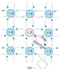
- p-type — trivalent dopants (acceptors): B, Al, In have valency 3. The atom bonds with three Si neighbours and has nothing to offer the fourth, leaving a bond vacancy — a hole. Each acceptor contributes one hole, so holes become the majority carriers: \(n_h \gg n_e\) (14.4) (NCERT, p. 9).
In all cases the crystal stays electrically neutral: the charge of the added carriers exactly balances the opposite charge of the ionised dopant cores. The electron and hole concentrations in thermal equilibrium obey the mass-action law:
\[ n_e n_h = n_i^2 \quad (14.5) \]
This holds for intrinsic and doped material alike (NCERT, p. 9-10).
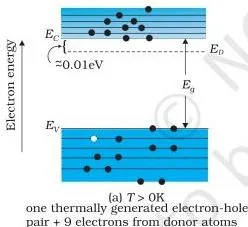
Doping also reshapes the energy bands. In n-type material, the donor level \(E_D\) sits slightly below the conduction band edge \(E_C\), and electrons need very little energy to step up into the conduction band.
In p-type material, the acceptor level \(E_A\) sits just above the valence band top \(E_V\), so electrons jump up to fill it, leaving holes behind (NCERT, p. 9-10).
n-type vs p-type: comparison table
| Feature | n-type | p-type |
|---|---|---|
| Dopant | Pentavalent — As, Sb, P | Trivalent — B, Al, In |
| Dopant role | Donor (gives one extra electron) | Acceptor (creates one hole) |
| Majority carriers | Electrons (\(n_e \gg n_h\)) | Holes (\(n_h \gg n_e\)) |
| Minority carriers | Holes | Electrons |
| Energy level position | \(E_D\) just below \(E_C\) | \(E_A\) just above \(E_V\) |
| Charge neutrality | Maintained — carrier charge balances the ionised dopant cores | |
Memory device — 5 → n, 3 → p. Pentavalent (5) dopants donate an electron and give an n-type semiconductor; trivalent (3) dopants leave a hole and give a p-type. Say it as “five frees an electron, three makes a hole” and you will never swap donors and acceptors in the exam.
Finding minority carriers (Example 14.2 pattern, NCERT p. 10): for a doped crystal, first note that thermally generated carriers are negligible beside doping-produced electrons, so set \(n_e \approx N_D\) (the donor concentration). Then apply the mass-action law: \(n_h = n_i^2 / n_e\). Stating \(n_e \approx N_D\) before substituting is the step that earns the mark.
The p-n Junction: Diffusion, Drift and the Depletion Region
Convert part of a thin p-type Si wafer into n-type by adding a small quantity of pentavalent impurity, and you create a p-region, an n-region and a metallurgical junction between them. Two processes shape the junction (NCERT, p. 11):
- Diffusion: holes are more concentrated on the p-side and electrons on the n-side, so holes diffuse p → n and electrons diffuse n → p, producing a diffusion current.
- Drift: every diffusing electron leaves behind an immobile positive ionised donor on the n-side, and every diffusing hole leaves an immobile negative ionised acceptor on the p-side. These immobile charges form the depletion region — about one-tenth of a micrometre thick — with an electric field pointing from the positive n-side to the negative p-side. The field sweeps carriers back, creating a drift current opposite to the diffusion current.

At first the diffusion current is large and drift small. As diffusion continues, the space-charge region widens, the field strengthens and drift grows until the two currents are exactly equal. At equilibrium the p-n junction carries no net current (NCERT, p. 12).
The n-side has lost electrons and is therefore positive relative to the p-side. This potential opposes further flow of carriers from n to p, so it is called the barrier potential \(V_0\) (NCERT, p. 12).
Can you just glue a p-slab to an n-slab to make a junction? No. Any slab, however flat, has surface roughness far larger than the inter-atomic spacing (about 2 to 3 Å), so atomic-level contact is impossible and the join behaves as a discontinuity for the charge carriers (NCERT, p. 12, Example 14.3).
Diode Behaviour: Forward Bias, Reverse Bias and Dynamic Resistance
A semiconductor diode is simply a p-n junction with metallic contacts at the two ends — a two-terminal device. In its circuit symbol the arrow points in the conventional direction of forward-bias current (NCERT, p. 12). Applying an external voltage V across the diode changes the equilibrium barrier in two opposite ways:
- Forward bias (p → positive, n → negative): the applied voltage opposes the built-in potential \(V_0\), so the effective barrier falls from \(V_0\) to \((V_0 – V)\) and the depletion layer narrows. Electrons cross from n to p and holes from p to n — minority carrier injection — raising the minority carrier concentration near the junction, which then diffuses onward. The resulting current is in the milliampere range (NCERT, p. 12-13).
- Reverse bias (n → positive, p → negative): the applied voltage adds to \(V_0\), so the barrier rises to \((V_0 + V)\) and the depletion region widens. Diffusion is suppressed; only a tiny drift of minority carriers across the junction remains. This reverse saturation current is a few microamperes, essentially independent of voltage until the breakdown voltage \(V_{br}\), where the current rises sharply (NCERT, p. 13-14).
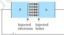
In forward bias the current stays almost negligible until the voltage crosses the threshold (cut-in) voltage — about 0.2 V for a germanium diode and 0.7 V for a silicon diode — after which the current rises exponentially with voltage (NCERT, p. 14).
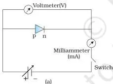
Experimentally, forward-bias current is large and is measured on a milliammeter, while reverse-bias current is tiny and needs a microammeter (NCERT, p. 14).
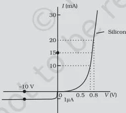
Because the diode’s V-I curve is not a straight line, we describe its resistance at a working point with the dynamic resistance — the ratio of a small change in voltage to the small change in current it produces (NCERT, p. 14):
\[ r_d = \frac{\Delta V}{\Delta I} \quad (14.6) \]
Rectifiers: Turning ac into dc with Diodes
The diode’s one-directional behaviour is put to work in a rectifier: a circuit that converts alternating voltage into unidirectional (pulsating) dc. When an ac voltage is applied across a diode in series with a load, current flows through the load only during the half-cycles in which the diode is forward biased (NCERT, p. 16).
- Half-wave rectifier: one diode in series with the load. Only the positive half-cycles reach the load, so the output is a train of half-sinusoid pulses. The output frequency equals the input frequency — 50 Hz in gives 50 Hz out (NCERT, p. 16; exercise 14.6).
- Full-wave rectifier: two diodes connected to a centre-tapped transformer secondary. Diode D₁ conducts when A is positive and D₂ when B is positive, so output appears across the load during both half-cycles. The output frequency doubles — 50 Hz in gives 100 Hz out. A four-diode bridge rectifier achieves the same without a centre tap (NCERT, p. 16-17).
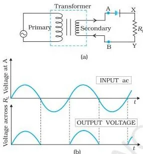
The rectified output is still pulsating, not steady dc. A capacitor filter connected across the load smooths it: the capacitor charges to the peak voltage during each pulse and then discharges through the load until the next pulse recharges it.
A large capacitance gives a large time constant (\(C \times R_L\)), a slower discharge and a smoother output that sits near the peak voltage — which is why power supplies use large capacitors (NCERT, p. 17).
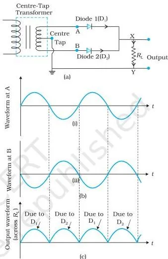
Real-world application — the phone charger: the adapter steps household 220 V ac down, a rectifier (often a bridge of four diodes) converts it to pulsating dc, and a large capacitor filter smooths it into steady dc that the battery can accept. It is exactly the half-wave/full-wave + filter chain described above.
Semiconductor Electronics Class 12 Physics Notes: Terms at a Glance
Every definition you may need to write in an exam, in one table:
| Term | Meaning | Example |
|---|---|---|
| Intrinsic semiconductor | Pure semiconductor with equal free electrons and holes | Pure Si, Ge |
| Extrinsic (impurity) semiconductor | Semiconductor whose conductivity is raised many times by doping | P-doped Si |
| Doping | Deliberate addition of a small amount of suitable impurity | Adding P to Si |
| Dopant | The impurity atom added | As, Sb, P, B, Al, In |
| Donor | Pentavalent impurity that contributes one extra conduction electron | As in Si (n-type) |
| Acceptor | Trivalent impurity that creates one hole | B in Si (p-type) |
| Hole | Bond vacancy with effective positive charge +q that behaves like an apparent free particle | Vacancy left when a covalent bond breaks |
| n-type | Doped material with electrons as majority carriers | Sb-doped Ge |
| p-type | Doped material with holes as majority carriers | In-doped Si |
| Depletion region | Space-charge region on either side of the junction, depleted of free charges, holding immobile ionised donors and acceptors | ~ one-tenth of a micrometre thick |
| Barrier potential | Junction potential (n positive relative to p) that opposes carrier flow | \(V_0\), overcome in forward bias |
| Minority carrier injection | Carriers crossing the junction under forward bias to become minorities on the other side | Electrons from n into p |
| Threshold (cut-in) voltage | Minimum forward voltage for significant current | ~0.2 V Ge, ~0.7 V Si |
| Reverse saturation current | Small, voltage-independent reverse current from drifted minority carriers | A few μA |
| Breakdown voltage | Critical reverse bias where reverse current rises sharply | \(V_{br}\) |
| Dynamic resistance | Ratio of a small voltage change to the small current change it causes | \(r_d = \Delta V / \Delta I\) |
| Rectifier | Circuit that converts ac to unidirectional pulsating dc | Half-wave, full-wave |
Formula Box: The Relations That Earn Marks
| Relation | Symbols and units | When to use it |
|---|---|---|
| \(n_e = n_h = n_i\) (14.1) | \(n_i\) = intrinsic carrier concentration (m⁻³) | Pure (intrinsic) semiconductor |
| \(I = I_e + I_h\) (14.2) | \(I_e\), \(I_h\) electron and hole currents (A) | Total conduction current in a semiconductor |
| \(n_e \gg n_h\) (14.3) | — | Identifies n-type material |
| \(n_h \gg n_e\) (14.4) | — | Identifies p-type material |
| \(n_e n_h = n_i^2\) (14.5) | all concentrations in m⁻³ | Finding minority carriers in a doped crystal |
| \(r_d = \Delta V / \Delta I\) (14.6) | \(r_d\) in Ω, \(V\) in V, \(I\) in A | Resistance at a point on the V-I curve |
| Effective barrier, forward: \((V_0 – V)\) | \(V_0\) built-in potential, \(V\) applied | Forward bias — barrier falls |
| Effective barrier, reverse: \((V_0 + V)\) | as above | Reverse bias — barrier rises |
Memory block — energy gaps: insulators \(E_g \gt 3\) eV, semiconductors 0.2–3 eV, metals \(E_g \approx 0\). Values: C 5.4 eV, Si 1.1 eV, Ge 0.7 eV (NCERT, p. 10; p. 19, summary point 11).
Worked Examples: Doping and Diode Resistance
These two calculation patterns cover nearly every numerical in the chapter. NCERT Examples 14.1–14.4 run the same methods with their own values.
Worked Example A: Electron and Hole Concentration in Doped Silicon
Method: doping adds far more electrons than thermal generation, so set \(n_e \approx N_D\), then apply the mass-action law \(n_e n_h = n_i^2\).
Step 1: Find the donor concentration.
A pure Si crystal has \(6 \times 10^{28}\) atoms m⁻³ and is doped with 2 ppm of pentavalent phosphorus (one P atom per \(10^6\) Si atoms):
\[ N_D = 2 \times 10^{-6} \times 6 \times 10^{28} = 1.2 \times 10^{23}\ \text{m}^{-3} \]
Step 2: Electrons dominate.
Given \(n_i = 1.5 \times 10^{16}\ \text{m}^{-3}\), the thermally generated electrons are negligible beside \(1.2 \times 10^{23}\), so:
\[ n_e \approx N_D = 1.2 \times 10^{23}\ \text{m}^{-3} \]
Step 3: Use (14.5) to find the holes:
\[ n_h = \frac{n_i^2}{n_e} = \frac{(1.5 \times 10^{16})^2}{1.2 \times 10^{23}} = \frac{2.25 \times 10^{32}}{1.2 \times 10^{23}} \approx 1.9 \times 10^{9}\ \text{m}^{-3} \]
Final answer: \(n_e \approx 1.2 \times 10^{23}\ \text{m}^{-3}\) and \(n_h \approx 1.9 \times 10^{9}\ \text{m}^{-3}\). Electrons are overwhelmingly the majority carriers (compare with NCERT Example 14.2, p. 10).
Worked Example B: Dynamic Resistance of a Silicon Diode
Method: the diode’s V-I curve is curved, so take two close points on it and use \(r_d = \Delta V / \Delta I\).
- Step 1: Read two forward-bias points from the curve: at \(I = 12\ \text{mA}\), \(V = 0.72\ \text{V}\); at \(I = 18\ \text{mA}\), \(V = 0.78\ \text{V}\).
- Step 2: Find the changes:
\[ \Delta V = 0.78 – 0.72 = 0.06\ \text{V}, \quad \Delta I = 18 – 12 = 6\ \text{mA} = 6 \times 10^{-3}\ \text{A} \]
Step 3: Substitute into (14.6):
\[ r_d = \frac{0.06\ \text{V}}{6 \times 10^{-3}\ \text{A}} = 10\ \Omega \]
Reverse check: at \(V = -8\ \text{V}\) the reverse saturation current reads \(I = -1.2\ \mu\text{A}\):
\[ r_d = \frac{8\ \text{V}}{1.2 \times 10^{-6}\ \text{A}} \approx 6.7 \times 10^{6}\ \Omega \]
Final answer: forward dynamic resistance 10 Ω; reverse resistance about \(6.7 \times 10^{6}\ \Omega\), nearly a million times larger. That huge ratio is why the diode conducts in one direction only (compare with NCERT Example 14.4, p. 14).
Common Mistakes Students Make in Semiconductor Electronics
| Mistake | Correct rule | How to check your answer |
|---|---|---|
| “Holes are real positively charged particles that move through the crystal.” | A hole is a bond vacancy with effective +q; bound electrons jump into it, so the hole only appears to move. | Both carriers contribute: \(I = I_e + I_h\) — free electrons carry current separately from holes. |
| “Forward bias raises the barrier.” | Forward bias lowers the barrier to \((V_0 – V)\); reverse bias raises it to \((V_0 + V)\). | p to positive, n to negative is forward — the barrier falls and depletion narrows. |
| “Donors are trivalent and acceptors are pentavalent.” | Pentavalent atoms donate an electron (n-type); trivalent atoms create a hole (p-type). | 5 → n, 3 → p. Five valence electrons donate; three leave a hole. |
| “In reverse bias the current keeps growing with voltage.” | Reverse current is essentially voltage-independent (a few μA), set by minority carrier concentration, until breakdown \(V_{br}\). | Reverse current changes almost nothing as V grows — only near \(V_{br}\) does it surge. |
| “\(n_e n_h = n_i^2\) means \(n_e = n_h\).” | Equality holds only in intrinsic material; in doped material one carrier dominates hugely. | In n-type \(n_e \gg n_h\) and \(n_h = n_i^2 / n_e\) is tiny. |
| “A silicon diode conducts well below 0.2 V.” | Each material has its threshold: ~0.2 V for Ge, ~0.7 V for Si. Below it, forward current is almost zero. | Check the cut-in voltage against the element — Si needs closer to 0.7 V. |
Exam Notes: Where the Marks Usually Sit in Chapter 14
These patterns come from the chapter’s own exercise structure (NCERT, p. 19-20) — not predictions, just the ideas the textbook itself tests:
- Energy-gap ranking: \(E_g\) for C > Si > Ge (exercise 14.3) — know the gap values cold.
- Minority carriers from \(n_e n_h = n_i^2\): writing \(n_e \approx N_D\) for n-type is the step that earns the mark (Example 14.2 pattern).
- Barrier direction wording: forward bias lowers the potential barrier (exercise 14.5) — state it the right way round.
- Dynamic resistance from the V-I curve: reading \(\Delta V\) and \(\Delta I\) between two points on the graph earns the marks (Example 14.4 pattern).
- Rectifier output frequency: 50 Hz in → 50 Hz out half-wave, 100 Hz out full-wave (exercise 14.6).
- n-type vs p-type identification: electrons majority + pentavalent dopant = n-type (exercise 14.1); holes majority + trivalent dopant = p-type (exercise 14.2).
For a similar last-night summary of the next chapter, see the Class 12 physics nuclei notes.
Quick Revision Recap: Semiconductor Electronics in One Page
| Idea | What to remember |
|---|---|
| Classification | Metals lowest resistivity, semiconductors intermediate, insulators highest |
| Energy gap | Insulator \(E_g \gt 3\) eV; semiconductor 0.2–3 eV; metal ≈ 0. C 5.4 eV, Si 1.1 eV, Ge 0.7 eV |
| Intrinsic | \(n_e = n_h = n_i\); holes are bond vacancies with effective +q |
| Extrinsic | Doping raises conductivity; n-type \(n_e \gg n_h\), p-type \(n_h \gg n_e\); \(n_e n_h = n_i^2\); crystal stays neutral |
| Junction | Diffusion vs drift; depletion region ~0.1 μm; barrier \(V_0\) opposes carrier flow |
| Bias | Forward lowers barrier \((V_0 – V)\), mA current; reverse raises barrier \((V_0 + V)\), μA current; cut-in 0.2 V Ge, 0.7 V Si |
| Rectifier | Half-wave 1 diode, \(f_{out} = f_{in}\); full-wave 2 diodes, \(f_{out} = 2 f_{in}\); capacitor filter smooths the dc |
That is Chapter 14 in one page. Browse the wider CBSE notes library and the Class 12 notes for your other subjects.
Frequently Asked Questions About Semiconductor Electronics
Why is carbon an insulator while silicon and germanium are semiconductors, even though all have four valence electrons?
Because their bonding electrons sit in different orbits. Carbon’s are in the 2nd orbit, silicon’s in the 3rd and germanium’s in the 4th, so ionisation energy is highest for carbon and lowest for germanium. At room temperature Si and Ge release a significant number of free electrons; carbon releases almost none (NCERT, p. 6, Example 14.1).
When a forward bias is applied to a p-n junction, does the potential barrier increase or decrease?
It decreases. Forward bias connects the p-side to the positive terminal, which opposes the built-in potential, so the effective barrier drops from \(V_0\) to \((V_0 – V)\) and the depletion region narrows (NCERT, p. 12, exercise 14.5).
What is the output frequency of a half-wave and a full-wave rectifier for a 50 Hz input?
Half-wave gives 50 Hz (one output pulse per cycle); full-wave gives 100 Hz (a pulse in every half-cycle, produced alternately by the two diodes) (NCERT, p. 16-17, exercise 14.6).
Do n-type and p-type semiconductors remain electrically neutral after doping?
Yes. The charge of the added majority carriers exactly balances the opposite charge of the ionised dopant cores, so the crystal maintains overall charge neutrality (NCERT, p. 9).
Why does a p-n junction diode conduct easily in forward bias but barely in reverse bias?
In forward bias the barrier falls to \((V_0 – V)\), so many carriers cross the junction and the current is in milliamperes. In reverse bias the barrier rises to \((V_0 + V)\), diffusion is suppressed and only a few minority carriers drift across — a few microamperes (NCERT, p. 12-13).
What are donor and acceptor impurities in a semiconductor?
Donors are pentavalent atoms (As, Sb, P) that contribute one extra conduction electron, making an n-type semiconductor. Acceptors are trivalent atoms (B, Al, In) that create one hole, making a p-type semiconductor (NCERT, p. 8-9).
Reference: NCERT Class 12 Physics textbook (Part II), chapter 14, Semiconductor Electronics: Materials, Devices and Simple Circuits.
Explore Class 12 Physics Notes
More for this chapter:
Class 12 Physics on LearnCBSE:
Related chapters: